
PCB is an indispensable part of electronic products, which carries electronic components and connects them, determining the performance and reliability of the whole product. In PCB design, choosing the right layer structure is crucial.
What are the advantages and considerations of multilayer PCB design?
I. Advantages of Multilayer PCBs
Multilayer PCB has many advantages over single or double layer PCB, mainly in the following aspects.
1. Dense wiring
Multilayer PCB can be wired through the inner layer, making the entire circuit more compact, shorter lines, reducing the impedance and delay in signal transmission, improving the circuit performance and speed.
2. Electromagnetic compatibility (EMC)
Multi-layer PCB design can effectively reduce the signal return path, reduce electromagnetic radiation, improve the anti-interference ability of the circuit, in line with the requirements of electromagnetic compatibility.
3. Power distribution
Multi-layer PCB can be reasonably arranged power and ground layer, providing more stable power distribution and good grounding effect, reducing power noise and power loss.
4. Packaging density
Multi-layer PCB design can accommodate more devices and components to improve packaging density, making the product more compact and lightweight, in line with the trend of modern electronic products.
II. Multilayer PCB design considerations
1. Inter-layer connection
The connection between different layers in the multi-layer PCB requires special attention, should choose the appropriate connection, such as through-hole (Via) or blind holes (Blind Via), etc., to ensure that the reliability of inter-layer connection and smoothness.
2. Layer isolation
Multi-layer PCB design, should be reasonable isolation of different signal layers and power layers, to avoid mutual interference, especially high-frequency signals and high-power signals to separate the layout, reduce crosstalk and noise.
3. Thermal management
In multi-layer PCB, the heat of the power layer may affect the stability of the signal layer, so it is necessary to consider good thermal management design, such as heat sink layout, selection of thermal components, etc., to ensure the thermal stability of the entire PCB.
4. Interlayer impedance control
Multilayer PCB design needs to control the impedance matching between layers, especially for high-speed transmission and high-frequency signal design, should choose the appropriate layer spacing and interlayer dielectric constants to ensure signal integrity and transmission quality.
5. Layer order planning
Multilayer PCB design, should be reasonable planning of the function and layout of each layer, such as high-frequency signal layer and high-speed transmission layer is placed in the inner layer, the power layer is placed in the outer layer, which is conducive to improving the performance and stability of the circuit.
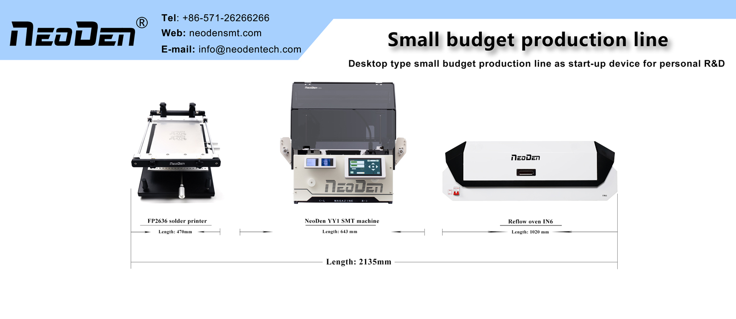
Features of NeoDen YY1 surface mount placement machine
1. Automatic nozzle changer help realizing nozzles changed flexibly.
2. Independent high-definition & high-speed dual vision recognition systems, as well as dual cameras for real-time display the working status.
3. Linear rail design for X, Y axis to ensure accuracy and stability, and reduce noise at the same time.
4. The newly-designed stick feeder with its compact shape, is perfectly compatible with the tape feeder system.
5. Comes with a high-definition capacitive touch screen, which can be adjusted up and down to meet the needs of different viewing angles and enhance the user experiences.
Post time: May-11-2024