SMT processing will appear some bad quality problems, such as standing monument, even tin, empty solder, false solder, etc.. There are many reasons for poor quality, if there is a need for specific analysis of specific problems.
Today with you to introduce the SMT printing even tin the causes and solutions.
What is SMT even tin?
From the literal meaning of the concept of tin can be well understood, is roughly the adjacent pads appear excess tin, the formation of connections, different pads or lines, by the excess tin connected together, also known as tin bridge.
The following is the SMT even tin reasons and improve countermeasures:.
1.Poor adhesion of solder paste
Solder paste is made of tin powder and flux combination, in the unpacked before use will be placed in the refrigerator, when the need to use, it is necessary to warm up and stir evenly in advance, appear even tin is due to the poor viscosity of the paste, may be back to temperature or stirring time is not sufficient.
Improvement measures
Before use, warm up the paste for more than 30 minutes and stir evenly until the paste does not break down. More and more large factories are now using intelligent solder paste management cabinets, which can effectively improve this problem.
2.Stencil opening is not precise enough
Stencil needs to be used for the patching, stencil is actually the pcb pad leak, need to be made with the pcb pad size and size, location, some stencil production defects, there may be too large openings, resulting in leakage of the amount of printed solder paste too much, there is a paste shift resulting in even tin.
Improvement countermeasures
The stencil needs to be carefully checked against the Gerber file, and the laser should be used to open the stencil, while the stencil opening (especially for pads with pins) should be a quarter smaller than the actual pad.
3.Solder paste printing machine printing, pcb board appears loose
PCB pads to print solder paste, the need to use solder paste printing machine, solder paste printing machine has a table for PCB solder paste printing and demoulding, in the PCB pad solder paste printing, PCB need to transfer to the table specified location, and the need for fixture fixed pcb board, if the transfer position deviation, fixture did not clamp pcb, will appear printing offset, produce even tin.
Improvement measures
When printing solder paste on a solder paste printer, you need to debug the program in advance so that the pcb transfer position is accurate, and the fixture should be regularly checked and replaced for maintenance.
The above factors, in order to avoid the occurrence of even tin and other bad quality, need to do a good job in the early proofing, but also in the back of the printing machine to add a SMT SPI machine detection, as far as possible to reduce the bad rate.
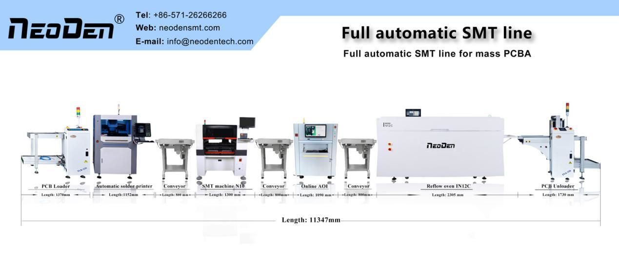
Features of NeoDen ND1 stencil printer
Transfer track direction Left – Right, Right – Left, Left – Left, Right – Right
Transmission mode Section-type track
PCB clamp mode
Software adjustable pressure of the elastic side pressure
Option:
1. Overall bottom suction chamber vacuum
2. Bottom multipoint partial vacuum
3. Edge lock clamping plate
Board support method Magnetic thimble, special work holding device (option: Grid-Lok)
Post time: Feb-02-2023

