News
-

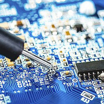
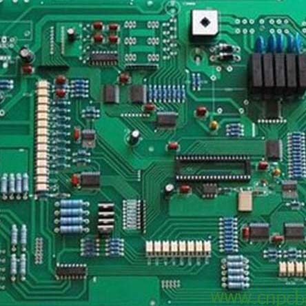
6 Tips for PCB Design to Avoid Electromagnetic Problems
In PCB design, electromagnetic compatibility (EMC) and the associated electromagnetic interference (EMI) have traditionally been two major headaches for engineers, especially in today’s circuit board designs and component packages continue to shrink, OEMs require higher speed systems. In th...Read more -

What Are The PCBA Cleanliness Inspection Methods?
Visual inspection method Using a magnifying glass (X5) or an optical microscope to PCBA, the quality of cleaning is assessed by observing the presence of solid residues of solder, dross and tin beads, unfixed metal particles and other contaminants. It is usually required that the PCBA surface mus...Read more -

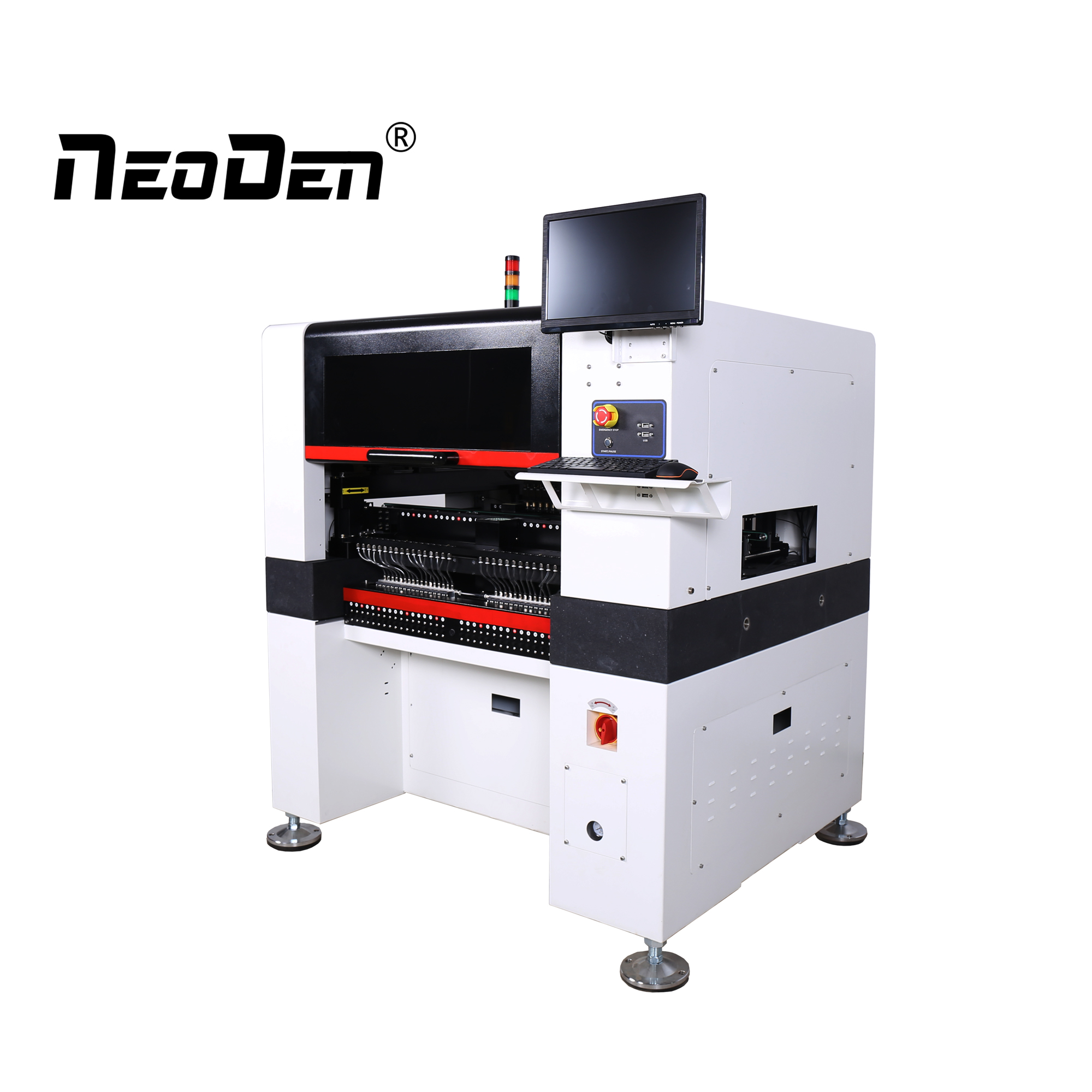
What Causes The Poor Suction of The SMT Machine?
We often encounter poorer and poorer suction capacity of the SMT machine in the process of using SMT machine for production and processing, sometimes even the suction is crooked, so what causes this situation? Many people think it is the quality of pick and place machine, in fact, it is not. The ...Read more -

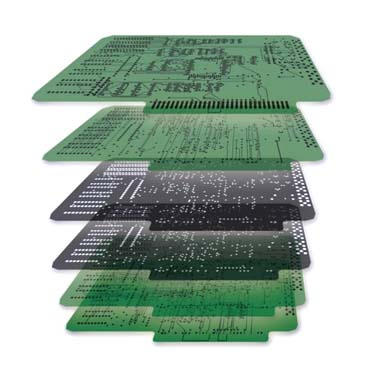
What Are The Requirements for PCB Board Press-fit Structure Design?
Multilayer PCB is mainly composed of copper foil, semi-cured sheet, core board. There are two types of press-fit structure, namely copper foil and core board press-fit structure and core board and core board press-fit structure. Preferred copper foil and core lamination structure, special plates ...Read more -

The Temperature and Humidity of PCB Board Storage and How to Store It?
with the development of electronic technology, circuit boards are widely used in various fields, almost all electronic devices have circuit boards. High-end automotive, aviation, medical electronics, common smart home, communication electronics, household appliances, etc. pcb board as a carrier o...Read more -

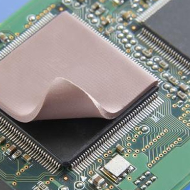
PCBA Thermal Pads Design Requirements
1. What is thermal pad The so-called thermal pads, refers to the bottom of the components with the metal side of the heat dissipation solder pads, usually relatively small power, mainly through the heat dissipation pads on the heat dissipation holes to the ground layer. In order to better heat di...Read more -

How to Improve The Production Efficiency of SMT Machine?
In the production line of SMT, the most important concern is often how to control production costs and improve production efficiency. This involves the problem of the SMT machine throwing rate. The high rate of SMD machine throwing material seriously affects the SMT production efficiency. If it i...Read more -

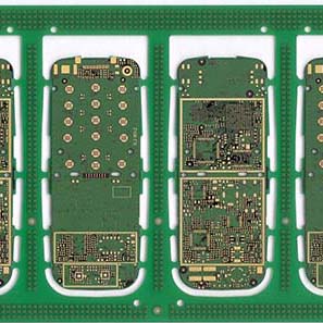
The 6 Steps of The Basic Process of Multilayer Circuit Board
The production method of multilayer boards is generally done by the inner layer graphics first, then by printing and etching method to make a single-sided or double-sided substrate, and into the designated layer between, and then by heating, pressing and bonding, as for the subsequent drilling is...Read more -

Reflow Oven Maintenance Methods and Precautions
Reflow Oven Maintenance Methods Before inspection, stop the reflow oven and lower the temperature to room temperature (20~30℃). 1. Clean the exhaust pipe:Clean the oil and dirt in the exhaust pipe with a cleaning cloth. 2. Clean dust and dirt from drive sprocket:Clean dust and dirt from drive spr...Read more -

What are the daily checks required for wave soldering machine?
What are the daily checks required for wave soldering machine? Check the flux filter and remove any excess flux residue. The flux filter is cleaned with water once a week, the inside of the extraction hood is cleaned weekly and the spray system is checked for uniformity of spray. The nozzle shoul...Read more -

Analysis of The Causes of Continuous Soldering with Wave Soldering
1. inappropriate preheating temperature. Too low a temperature will cause poor activation of flux or PCB board and insufficient temperature, resulting in insufficient tin temperature, so that the liquid solder wetting force and fluidity becomes poor, adjacent lines between the solder joint bridge...Read more -

Reflow Oven Process Requirements
Reflow soldering machine technology is not new to the electronics manufacturing sector, as the components on the various boards used within our computers are soldered to the circuit boards using this process. The advantages of this process are that the temperature is easily controlled, oxidation ...Read more

